Here, we work to find the best detector designs that maximise image information capacity for a given beam energy and/or sample thickness. Design features include the sensor material, detection algorithm, signal speed and radiation tolerance.
Electron Detector Development
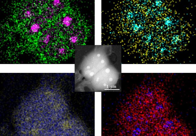
Atomic resolution imaging with electrons causes sample damage. The information per unit of damage is dependent on sample thickness and beam energy.
Technical detail
Forming electron beam images requires conversion of the high electron energy (partially or fully) into solid-state excitations and locating the arrival on a semiconducting chip. The faster the detector can sense and report the arrivals, the quicker the image acquisition and the faster the microscope throughput. Current on-the-market sensor readout times are of the order of microseconds (one millionth of a second). The time taken to bring an electron to a stop (by the sensor), or register its passage, is a few picoseconds or less (one millionth of a millionth of a second). The design of the sensor, the detecting electronics and signal handling can, in principle, shrink this disparity in time. Doing this for different electron beam energies (optimized for sample type) is the final hurdle.
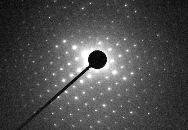
Characterising candidate detector system requires measurement of the image acuity (image sharpness) and its responsiveness to the electron – the modulation transfer function (MTF) and the detective quantum efficiency (DQE), respectively. We use Crewe, with its customisable detector chamber and imaging capability across a broad range of electron beam energies, to test candidate sensor designs, often in conjunction with STFC and the CERN detector development groups. Such measurements require controlled electron beam fluxes, and carefully shaped sensor illumination geometries to measure the electron-sensor response.
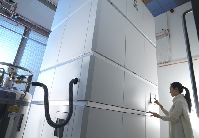
The large space underneath the microscope allows us to mount several detectors simultaneously without affecting the imaging capability for the day-to-day use. For example, this microscope is being configured for three detectors with very different energies:
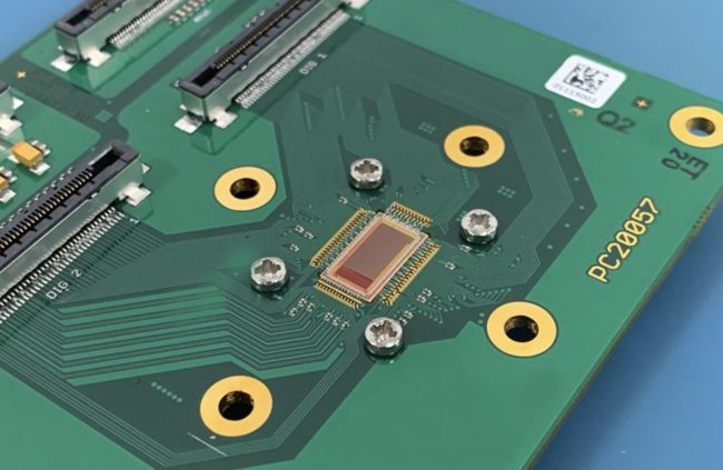
At 300 kV (nominal microscope energy) a Gatan K2 camera is used. Its small pixel size (7 μm) and large number of pixels (3836 ×3706) with back thinned monolithic active pixels (MAPs) provides sharp imaging for single particle analysis, electron tomography and micro-electron diffraction.
Based on the charged particle tracking detectors at the large hadron collider, the Timepix 4 camera with a 300 μm thick sensor provides event-driven detection. Event-driven detection means that the arrival of each electron is reported as a single 64-bit data output registering the location and time of arrival to within 200 picoseconds. The array size is 512 × 448 pixels with 55 μm square pixels. Maximum electron flux is about 10 pA before pile-up artefacts become apparent. It is used for extremely low-dose applications such as micro-electron diffraction.
Finally, a STFC/QD C100 camera based on MAPs device is used for 100 keV electrons. Like the Timpepix4, it has 55 μm square pixels that match the approximate interaction volume of 100 keV electrons in silicon. The sensor is 2048 × 2048 pixels and has a readout speed of 2 kHz. This sensor has been developed in conjunction with Richard Henderson and Chris Russo at the Laboratory for Molecular Biology at Cambridge.
Project Team


Collaborators


Platforms
Contact information


PhD Studentships
Find out more